Privacy statement: Your privacy is very important to Us. Our company promises not to disclose your personal information to any external company with out your explicit permission.
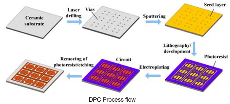
The preparation process of DPC Ceramic Substrate is shown in the figure. First, a laser is used to prepare through holes on the Blank Ceramic Substrate (the aperture is generally 60 μm ~ 120 μm), and then the ceramic substrate is cleaned by ultrasonic waves; the magnetron sputtering technology is used to deposit metal on the surface of the ceramic substrate. Seed layer (Ti/Cu), and then complete the circuit layer production through photolithography and development; use electroplating to fill holes and thicken the metal circuit layer, and improve the solderability and oxidation resistance of the substrate through surface treatment, and finally remove the dry film, engraving Etch the seed layer to complete the substrate preparation.

The front end of DPC ceramic substrate preparation adopts semiconductor micromachining technology (sputter coating, lithography, development, etc.), and the back end adopts printed circuit board (PCB) preparation technology (pattern plating, hole filling, surface grinding, etching, surface processing, etc.), the technical advantages are obvious.
Specific features include:
(1) Using semiconductor micromachining technology, the metal lines on the ceramic substrate are finer (the line width/line spacing can be as low as 30 μm ~ 50 μm, which is related to the thickness of the circuit layer), so the DPC substrate is very suitable for alignment accuracy Microelectronic device packaging with higher requirements;
(2) Using laser drilling and electroplating hole filling technology to achieve vertical interconnection between the upper and lower surfaces of the ceramic substrate, enabling three-dimensional packaging and integration of electronic devices and reducing device volume, as shown in Figure 2( b);
(3) The thickness of the circuit layer is controlled by electroplating growth (generally 10 μm ~ 100 μm), and the surface roughness of the circuit layer is reduced by grinding to meet the packaging requirements of high temperature and high current devices;
(4) Low temperature preparation process (below 300°C) avoids the adverse effects of high temperature on substrate materials and metal wiring layers, and also reduces production costs. To sum up, the DPC substrate has the characteristics of high graphic accuracy and vertical interconnection, and is a real Ceramic PCB Substrate.
However, DPC substrates also have some shortcomings:
(1) The metal circuit layer is prepared by electroplating process, which causes serious environmental pollution;
(2) The electroplating growth rate is low, and the thickness of the circuit layer is limited (generally controlled at 10 μm ~ 100 μm), which is difficult to meet the needs of large Current power device packaging requirements.
At present, DPC Ceramic Substrates are mainly used in high-power LED packaging.
LET'S GET IN TOUCH

Privacy statement: Your privacy is very important to Us. Our company promises not to disclose your personal information to any external company with out your explicit permission.

Fill in more information so that we can get in touch with you faster
Privacy statement: Your privacy is very important to Us. Our company promises not to disclose your personal information to any external company with out your explicit permission.